Fabrication
3.1 Overview of Fabrication Steps
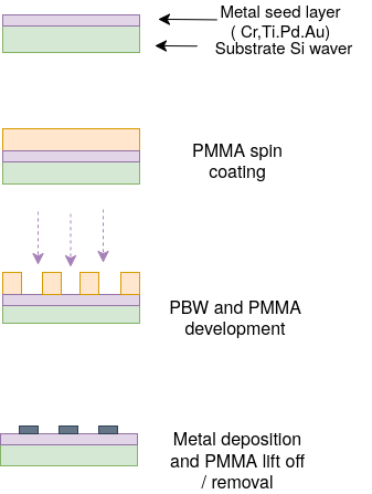
An updated overview of the fabrication process is shown above, incorporating the full material stack decisions described in Section 2.4. The four-stage sequence of spin coating, PBW exposure, metal deposition, and lift-off is followed for each sample.
3.2 Simulations of P-beam in PMMA
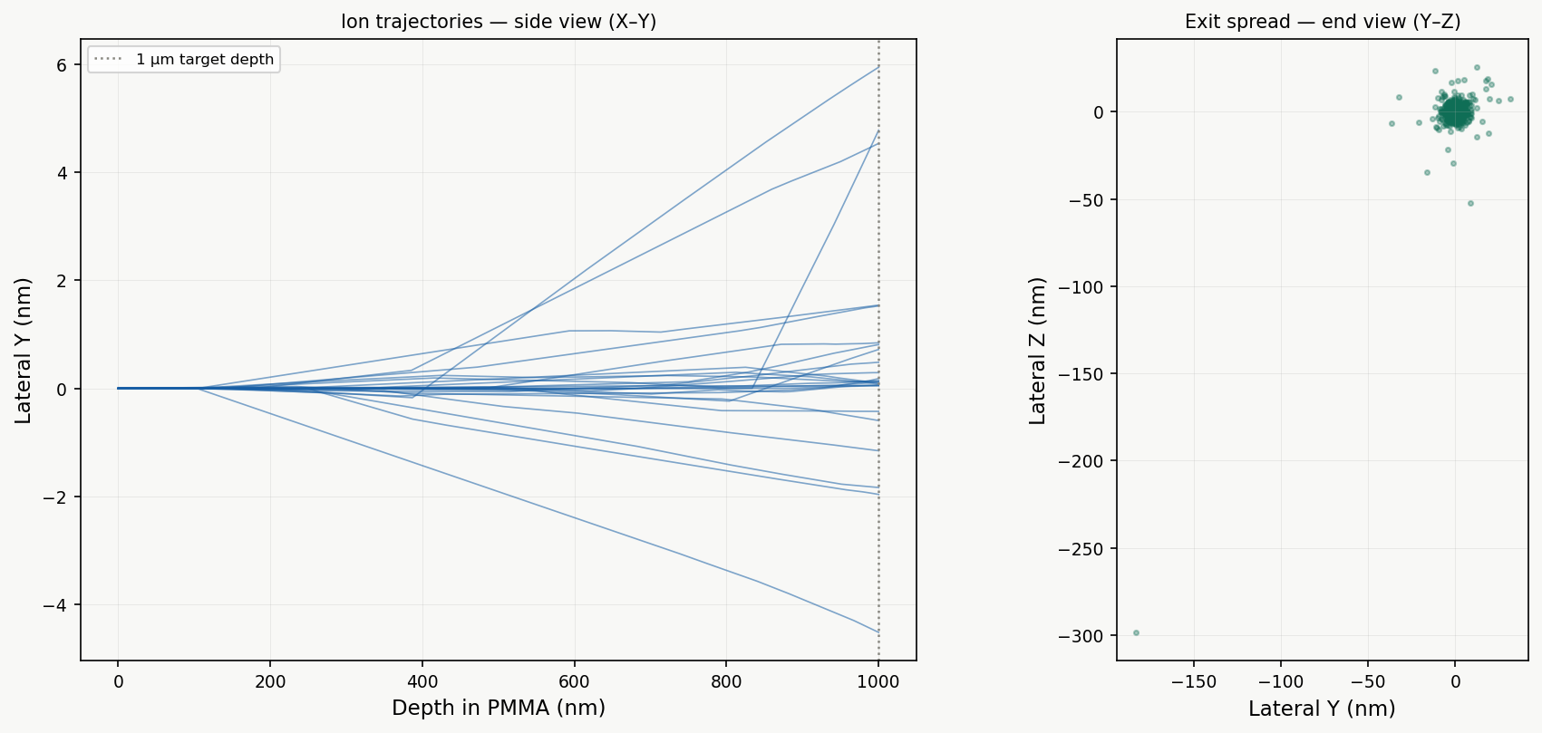
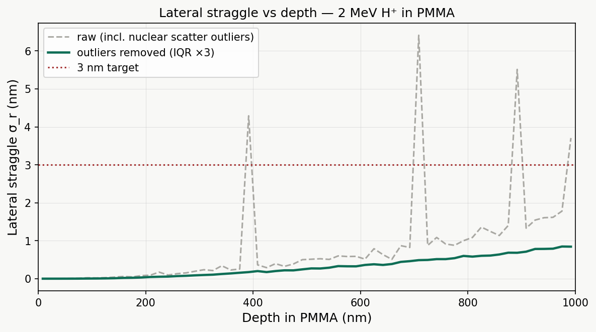
To better understand how the proton beam behaves inside the PMMA, SRIM Monte Carlo simulations were run. These simulations predict the lateral spread of the beam as a function of depth, which directly determines how vertical the fabricated edges will be.
Two parameters were fixed for the simulation. Energy was set to 2 MeV to match the physical beam energy available at the CIBA facility. Depth was set to 1 µm, corresponding to the maximum PMMA thickness used in this fabrication process.
Key findings:
The simulation confirms that at 2 MeV, the protons pass through the 1 µm PMMA layer without stopping, ensuring the full feature height can be patterned. The lateral straggle at the exit depth is only 0.81 nm, demonstrating that the proton beam maintains much tighter lateral precision than conventional EBL (see Section 1.2).
Occasional spikes in the trajectory data represent rare instances where a proton undergoes a large-angle nuclear scatter event. These are statistical outliers and do not affect the overall sharpness of the final feature.
Theoretical Sidewall Angle
The lateral straggle σ(z) from SRIM gives the standard deviation of the beam’s lateral spread at depth z. The edge transition width at that depth is related to σ by:
\[f(z) = 2\sqrt{2\ln 2} \cdot \sigma(z) \approx 2.355\,\sigma(z)\]where f is the FWHM of the dose profile across the feature edge, the same parameter extracted from SEM measurements in Section 2.5.1. The theoretical sidewall angle at the full feature depth h is then:
\[\theta = 90° - \arctan\!\left(\frac{f(h)}{h}\right) = 90° - \arctan\!\left(\frac{2.355\,\sigma(h)}{h}\right)\]3.3 Spin Coating the Wafer and Development
Spin Coating
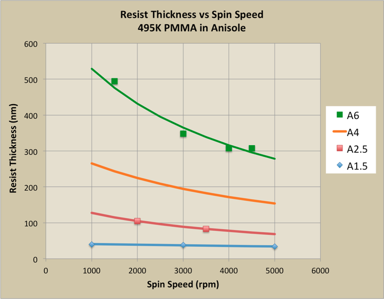
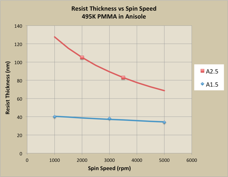
Film thickness is governed by two parameters: the concentration (viscosity) of the resist solution and the spin speed [1]. Higher spin speeds and lower concentrations produce thinner films, following an approximate inverse power-law relationship.
A key design constraint is that the PMMA thickness must be at least five times greater than the intended metal deposition thickness. This ratio is required for two reasons: it ensures sufficient structural integrity of the resist walls during development and metal deposition; and it prevents metal from overflowing the resist sidewalls, a phenomenon known as mushrooming, where excess metal forms a cap over the resist that prevents clean lift-off. Since the metal deposition height varies per sample, the curves above show the range of PMMA thicknesses used across the project.
Pre-bake and Post-bake
After spin coating, the wafer is placed on a hotplate for a soft bake, typically at 180 °C for 60 to 90 seconds [1] [3]. The pre-bake serves two purposes: it drives off residual solvent (anisole) from the film, which would otherwise cause the resist to remain tacky and deform during handling; and it densifies and hardens the film, improving adhesion to the substrate and reducing unwanted swelling during development. Baking above approximately 125 °C is avoided as PMMA begins to flow and reflow at elevated temperatures, rounding the resist edges [1].
Development and Lift-off
Development is performed after PBW exposure. The wafer is immersed in DI water:IPA (7:3) developer, which selectively dissolves the chain-scissioned PMMA in the exposed regions while leaving the unexposed resist intact [1] [2]. The sample is then rinsed in fresh IPA and dried with a nitrogen gun to stop development. Following metal deposition, the remaining PMMA is removed by immersion in acetone, lifting off the metal on top of the resist and leaving only the metal deposited directly onto the silicon substrate.
3.4 P-beam Structure
This section covers the general proton beam components that must be adjusted or calibrated before and during PBW, in order to control the spot size.
Before patterning begins, the beam focus is verified by scanning across a resolution standard. By fitting the resulting signal to an error function, the beam FWHM is extracted to confirm the beam is at its sharpest.
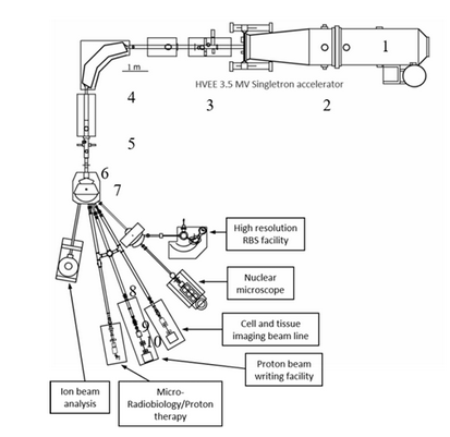
The Proton Beam Writing (PBW) facility at CIBA is built around a 3.5 MV Singletron accelerator (HVEE), which generates the focused MeV proton beam required for high-resolution lithography [4] [5]. To achieve sub-10 nm precision, the system refines the beam through several critical stages.
1. Beam Generation and Refinement
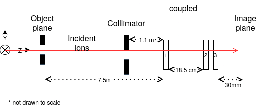
Protons are produced from hydrogen gas, accelerated to 2 MeV, and filtered by a 90° analysing magnet. This ensures a clean beam before it is directed to the end station via a switching magnet. Two apertures then define the beam geometry [4]: the objective aperture (8 x 4 µm²) defines the virtual source size, and the collimator aperture (30 x 30 µm²) limits angular divergence to approximately 3 µrad.
2. The Oxford Triplet (Demagnification)
Focusing is achieved using a spaced Oxford triplet of magnetic quadrupole lenses in a converging-diverging-converging (CDC) configuration. Since a single quadrupole focuses in one plane while defocusing the other, this triplet is essential for a symmetric spot focus [4]. With an object-to-lens distance of 7.5 m and an image distance of 30 mm, the system achieves a demagnification of 857x in X and 130x in Y, resulting in a minimum spot size of 9.3 x 32 nm².
3. Stability and Calibration
At these scales, chromatic aberration is the primary limit on spot size. To maintain sub-10 nm resolution, the accelerator requires a stability of approximately 10 ppm [4]. Before writing, the beam focus is verified by scanning across a resolution standard. The transmitted or secondary electron signal produces a complementary error function profile, which is fitted to extract the beam FWHM (as discussed in Section 2.5). Once focused, electrostatic scanners and stage movement are used to raster the beam over the resist [5].
The interactive simulation above demonstrates how varying the beam parameters affects the spot size.
4. Strategic Focal Plane Positioning
The sample stage can be adjusted along the beam axis with 1 µm accuracy. Because the beam converges to a minimum waist at the focal point and diverges on either side, the effective spot size depends on the defocus distance and the cone half-angle. By varying the focal plane, beam divergence at depth can be partially compensated, counteracting lateral spread at greater resist depths.
System Specifications Summary
| Parameter | Value |
|---|---|
| Accelerator | 3.5 MV Singletron (HVEE) |
| Beam Energy | 2 MeV protons |
| Beam Half-Divergence | ~3 µrad |
| Lens Configuration | Spaced Oxford triplet (CDC) |
| Demagnification (X / Y) | 857 / 130 |
| Stage Accuracy (Z-axis) | ~1 µm |
| Power Supply Resolution | 2 ppm (Bruker) |
3.5 Metal Deposition Characteristics
| Material | Deposition Technique | Melting Point (°C) | Conductivity (S/m) | Rationale |
|---|---|---|---|---|
| Au | Magnetron sputtering | 1064 | 4.52 x 10⁷ | Excellent SEM/TEM contrast; chemically inert; well-established PVD process; lift-off compatible |
| Pd | E-beam evaporation | 1554.9 | 9.5 x 10⁶ | Good contrast; chemically stable; used for X-ray zone plates and resolution standards; higher melting point limits substrate heating risk |
| Cr | Magnetron sputtering | 1907 | 7.9 x 10⁶ | Deposited as adhesion buffer layer beneath Au; strong bonding to Si oxide; reduces Au-Si lattice mismatch stress |
| DLC | FCVA | N/A (amorphous) | ~10⁻³ to 10² (sp²/sp³ dependent) | Smoother surface than sputtered Au; low roughness improves specular signal retention |
The metals selected for this project were chosen on the basis of the criteria established in Section 2.4: lift-off compatibility, electron scattering contrast, chemical stability, and lattice mismatch, alongside the practical constraint of cleanroom availability at CIBA.
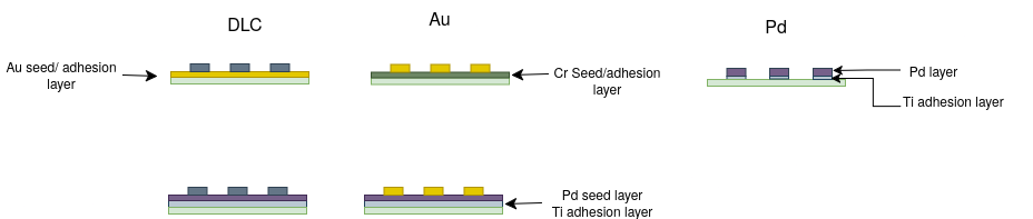
Gold (Au) was selected as the primary structural metal due to its well-established compatibility with magnetron sputtering workflows at CIBA, its high electron detector backscatter contrast, and its chemical inertness. Chromium (Cr) was included as an adhesion buffer layer beneath Au, exploiting its strong bonding to native silicon oxide and its ability to reduce internal stress arising from the Au-Si lattice mismatch. Palladium (Pd) was evaluated as an alternative primary metal due to its good chemical stability and higher melting point, which reduces the risk of substrate heating during e-beam evaporation. Diamond-like carbon (DLC) was investigated as a candidate surface coating to improve roughness performance after surface uniformity concerns with sputtered Au were observed. Titanium (Ti) was later introduced as an alternative adhesion layer to Cr, offering improved interfacial bonding for Pd-based stacks.
Fabricated Samples Composition
| Sample | Cr | Ti | Pd | Au | DLC |
|---|---|---|---|---|---|
| 1: Au/Cr/Si | 2 nm | 30 nm | |||
| 2: Au/Pd/Ti/Si | 2 nm | 2 nm | 20 nm | ||
| 3: DLC/Si | 5 nm | ||||
| 4: DLC/Au/Si | 2 nm | 10 nm | |||
| 5: DLC/Pd/Ti/Si | 2 nm | 10 nm | |||
| 6: Pd/Ti/Si | 2 nm | 100 nm |
Importantly not all the samples where tested using the SEM for sidewall characterization
The DLC and Au samples was made and tested for surface roughness and to compared relative electron counts, when scanned with the p-beam
The Pd sample (Sample 6) was the only sample tested with the SEM, this is because the Au surface was too rough and the DLC surface although smoother was too thin a layer to be properly calculated using the line fit method
Pd Fabrication - Key Structural Diffrences
Unlike the Au and DLC samples where the Ti adhesion layer was deposited across the entire Si surface prior to PMMA coating, the Pd sample followed an inverted process, PMMA was spun first, followed by PBW exposure, then Pd/Ti deposition into the developed apertures. As a result, the Ti adhesion layer is confined solely to the footprint of the Pd features and is absent from the surrounding Si surface.
Since the metal is deposited into an already-developed PMMA mould, any edge roughness or warping originates entirely from the PBW exposure or PMMA processing steps rather than from seed layer non-uniformity
| ← Prev: Methodology | Next: Results and Analysis → |
References
- Microchem / Kayaku Advanced Materials, "PMMA Data Sheet," 2019. Available: kayakuam.com
- J. A. van Kan, P. Malar, and A. B. H. Tay, "Resist materials for proton beam writing: a review," Appl. Surf. Sci., 2014. DOI: 10.1016/j.apsusc.2014.04.147
- University of Chicago Pritzker Nanofab, "NANO 495 PMMA process," 2024. Available: pnf.uchicago.edu
- S. Raman, Y. Yao, and J. A. van Kan, "Automatic beam focusing in the 2nd generation PBW line at sub-10 nm line resolution," Nucl. Instrum. Methods Phys. Res. B, vol. 348, pp. 22–26, 2015. DOI: 10.1016/j.nimb.2014.12.066
- J. A. van Kan, P. Malar et al., "Proton beam writing nanoprobe facility design and first test results," Nucl. Instrum. Methods Phys. Res. A, 2011. DOI: 10.1016/j.nima.2010.12.011